A 95MHz 32-bit Pipelined RISC-V Processor
This is a two-stage pipelined RISC-V processor with a limited instruction set. I created this as part of my Design of Computing Systems (ENGN1640) class, which I took in my junior spring at Brown.
Previously in the class, we had created a single-cycle RISC-V processor with no pipelining. That means the processor fully completes one instruction (reading it from instruction memory, copying the relevant memory out of the stack into a register, doing the calculation, and storing the result) before embarking on the next one. As one can imagine, this is fairly inefficient. The goal was to improve the processor by at least 15% using pipelining.
This document covers the general structure of the processor, the pipelining strategy I selected, and an example program (Sokoban). Sokoban was created in collaboration with my lab partner, Yash Vora.
Since this is still used as an assignment in this class, I will avoid talking about many of the low-level design decisions or actual RISC-V code! These are the broadstrokes.
General Remarks
This is a two-stage pipelined processor which handles the following RISC-V instructions:
| Instruction | Meaning |
| add | Adds two registers and stores the result to a register. |
| addi | Adds a register and a given constant and stores the result to a register. |
| sub | Subtracts one register from another and stores the result to a register. |
| and | Returns bitwise AND of two registers. |
| or | Returns bitwise OR of two registers. |
| slli | Shifts a register left by some constant. |
| mul | Multiplies two registers together and stores the result to a register. |
| sw | Store a register to an address on the stack. |
| lw | Loads an address from the stack to a register. |
| beq | Jump to a given instruction if two registers are equal. |
| bne | Jump to a given instruction if two registers are not equal. |
| jal | Jump to a different constant location in instruction memory. |
| jalr | Jump to a different location in instruction memory, dictated by a register (usually the stack pointer). |
| halt | (Not native RISC-V) Halt execution. |
Adding more instructions would have been fairly trivial; the limited instruction set was dictated by the professor.
Implementation of the processor was done through Altera’s Quartus, a programmable logic device design software. Functionality was tested through deployment on an FPGA board.
Timing Statistics
| Stat | Value |
| Max. Operating Frequency | 95MHz |
| Clock Period | 10.53ns |
| Duty Cycle | 20% |
| CPI | 1 (!) |
Memory and Stack
The instruction memory can contain up to 232 - 1 instructions (although this can be readily extended). The first entry in instruction memory (address 0) is hardcoded to be 0 and should not be overwritten (or undefined behavior will be observed). The first instruction should be written to the instruction memory location 1.
The stack contains 256 32-bit entries, placed at intervals of 4 words. Stack access is word-aligned (that is, the stack pointer will access at multiples of 4.) If sp is not a multiple of 4, the value will get rounded down to the nearest multiple of 4 before access. The stack pointer (x2) is initialized to 1020, which accesses the last (255th) entry.
Pipelining and Branch Resolution
Branch resolution occurs in the first stage (IF-ID-EX), bypassing the need for any fancy branch-decision logic or stage flushing. The program counter is always supplied with the correct next instruction within the first cycle.
The CPI is so low because the processor is only two-stage; unlike many other pipelined processors, the chip never needs to stall to avoid load-use or compute-use hazards. Writing from data memory into the register occurs before register reads, bypassing load-use hazards, and forwarding from the ALU output bypasses compute-use hazards. By sacrificing some frequency, we get an insanely fast CPI (equivalent to a single-cycle processor).
This was a conscious decision early in the design process and not one I made trivially. By only dividing the CPU into two stages, one fails to compartmentalize some fairly chunky processes. If these had not been implemented efficiently, my overall frequency would not have been reduced enough, leading to an ineffective processor even with the low CPI. It would have been equally valid to, say, implement a four-stage processor, or even split the EX stage (since the ALU contributes the greatest delay here). But that would have added complexity with hazard detection and forwarding, which I ultimately opted to avoid. I ended up making some small optimizations to the ALU in order to boost the overall frequency.
Registers
Several registers are reserved for internal use or FPGA I/O:
| Register | Use |
| x1 | register address (ra) |
| x2 | stack pointer (sp) |
| x27 | reserved for I/O (button 0 - “down”) |
| x28 | reserved for I/O (button 1 - “up”) |
| x29 | reserved for I/O (button 2 - “left”) |
| x30 | reserved for I/O (button 3 - “right”) |
| x31 | reserved for I/O (switch) |
The last five registers are constantly updated by an I/O controller to reflect the status of the input devices, and can be referenced by the program.
Writing to the Screen
Writing to the screen was handled by a VGA buffer module and video controller (which were supplied). A specific RAM module (with larger addresses than the stack) can be written to with an ASCII character and 12-bit RGB information, which would then be rendered by the controller based on a set of stored bitmaps.
Floorplan
Modules
The processor contains eight total modules:
- Instruction Memory (instruction_memory): where the machine code for instructions are stored, and the program counter is stored and updated.
- Control (control): where the control bits for other modules are set based on the current instruction.
- ALU Control (alu_control): an additional control module for setting the ALU operation code.
- Registers (registers): where the registers are stored.
- Immediate Generation (imm_gen): where 32-bit immediate values are generated based on the current instruction.
- ALU (alu): the arithmetic logic unit.
- Data Memory (ram:data_memory): where the memory for the stack is stored.
- I/O Controller (io_control): polls the input buttons and switches, and sets reserved registers based on their current values.
Including the PLL (which generates the 95MHz clock with a 20% duty cycle from the FPGA’s onboard clock), and the VGA buffer/video controller, this makes ten modules. There are also various MUXes to select inputs for different modules based on control bits (set by the control module).
Resource Consumption
| Resource | Definition | # |
| ALM | A collection of basic logic elements in the FPGA. | 1203 |
| LAB | Higher-order category of a group of logic elements. Roughly equivalent to overall floorplan. | 73 |
| ALUT | A collection of basic logic elements in the FPGA. | 1482 |
| Logic register | Any kind of register, including those used to handle pipelining. | 1304 |
| PLL | Unit to generate the non-standard clock frequency. | 1 |
| Memory blocks | Blocks of memory used for instruction and stack. | 4 |
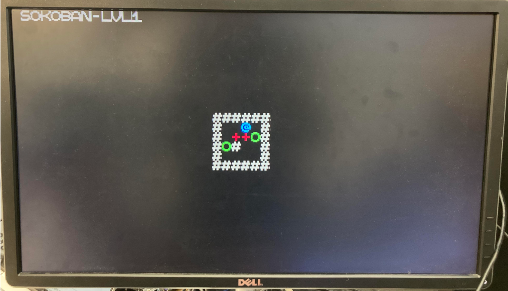
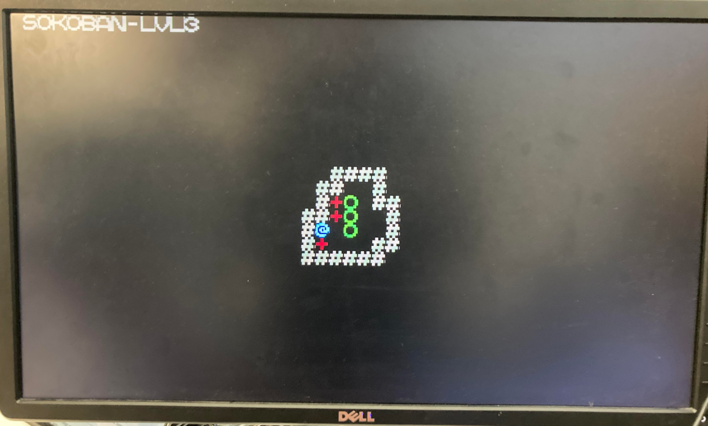
Example Program: Sokoban
This is the example program written in RISC-V assembly code, in collaboration with a partner, Yash Vora. It’s an implementation of the classic Japanese puzzle game Sokoban (倉庫番, meaning “warehouse keeper”), where the player pushes blocks around a level to get them onto specific tiles (referred here as “pressure plates”). A level is completed when every pressure plate is covered by a box. A player can push a box as long as the space behind it is empty (i.e. not filled with a box or a wall). This leads to surprisingly challenging levels and emergent gameplay! Our Sokoban contains three implemented levels, as an example; the assembly code can be readily extended to include arbitrarily many.
Controls
Four buttons are used as movement; up, down, left, and right.
The switch is used a level reset; setting it to ON and then OFF again will reset the current level to its initial condition.
Movement and Rendering
When a player attempts to move in a direction, the outcome depends on the tiles which are located in that direction:
- What’s the next tile in that direction?
- Wall –> do nothing
- Empty, plate –> move!
- Block –> What tile is behind that block?
- Wall, block –> do nothing
- Empty, plate –> move!
Only one sprite may be rendered on a tile. The sprites are rendered according to the following priority:
- Wall: #
- always grey
- Box: +
- if on a pressure plate –> green
- otherwise –> brown
- Player: @
- if on a pressure plate –> green
- otherwise –> blue
- Pressure plate: O
- always green
The top of the screen says SOKOBAN - LEVEL N, where N is the current level.
Winning and Levels
A player beats their current level when every pressure plate is covered by a block. As currently implemented, each level has the same number of plates and blocks; however, it is theoretically possible for a level to have more blocks than plates, and indeed the current setup supports this. In that case, all the game requires is for every plate to be covered; not for every block to be on a plate.
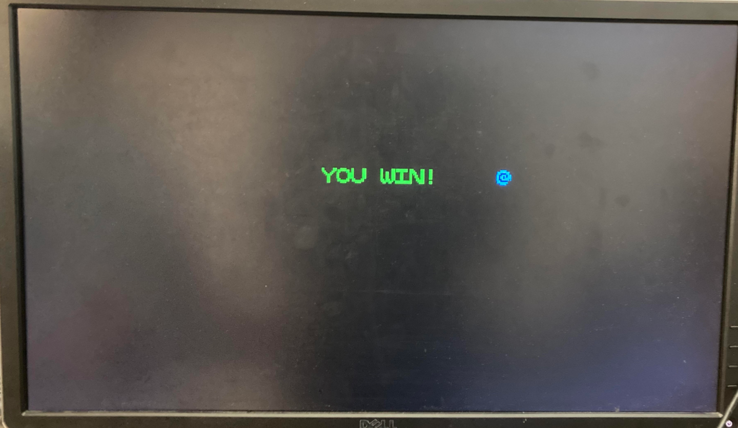
When a level is beaten, the game wipes the screen and then renders the next level for them to play. The player advances sequentially through levels (so level 1 first, then level 2, then level 3). A winscreen is displayed after the second level (to demonstrate functionality); but hitting the reset switch on the winscreen will display more levels!
Register Descriptions
- x1: register address
- x2: stack pointer
- x3: temporary used for storage in render (can be re-used)
- x4: temporary used for storing words in render (can be re-used)
- x5: temporary used for memory location storage in render (can be re-used)
- x6: temporary used for vga location storage in render (can be re-used)
- x7: “height” of the play area
- x8: total volume of the play area
- x9: the vga storage location
- x10: wall sprite
- x11: player sprite
- x12: player memory location
- x13: player vga location
- x14: temporary used for storage in render
- x15: temporary used for checking memory locations
- x16: box sprite
- x17: bitflags for button presses
- x18: intermediate for calculating button press bitflags
- x19: plate sprite
- x20: player-on-plate sprite
- x21: box-on-plate sprite
- x22: current level counter
- x23: temporary used for movement
- x24: temporary used for win-checking
- x25: “negative height” of the play area (used for movement)
- x26: temporary used for rendering top bar
- x27: reserved for I/O – KEY0
- x28: reserved for I/O – KEY1
- x29: reserved for I/O – KEY2
- x30: reserved for I/O – KEY3
- x31: reserved for I/O – SW0
Images